SILICON RIVER
CHOREOGRAPHING BANGLADESH’S SEMICONDUCTOR RENAISSANCE

News Desk
20 June 2026, 19:49
From an asset-light design ecosystem to a billion-dollar global technology powerhouse: A roadmap for the future of Bangladesh
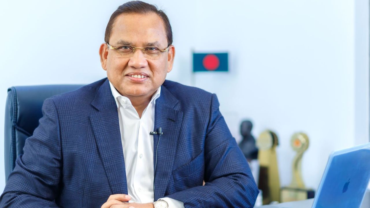
To map out how the nation intends to transition from a participant to an orchestrator, TechWorld Bangladesh sat down with M. A. Jabbar, the vision leader steering the country’s silicon ambitions. In this deep-dive interview, he lays out the “War Room” strategies, regional corridors, and the cultural transformation required to turn Bangladesh into an indispensable node in the global silicon value chain.
The $2 Trillion Opportunity
TW: Global semiconductor sales are projected to hit $2.06 trillion by 2032. Which high-growth sub-sectors should Bangladesh target to ensure we are leaders, not just participants?
MAJ: Bangladesh must decide early whether it wants to be a follower of trends or a setter of them. The global semiconductor industry, heading toward $2.06 trillion, is not simply expanding—it is being redefined by those who think deeply, not those who move quickly without direction.
We see six strategic sub-sectors where Bangladesh can lead with intention.
- First, AI-centric chip design (ASICs), particularly for edge intelligence, low-power AI, and domain-specific accelerators. This is where intelligence meets silicon, and where future economic value will concentrate.
- Second, advanced packaging and OSAT, including 2.5D and 3D integration, where performance is increasingly unlocked not by smaller transistors alone but by smarter integration.
- Third, digital twin systems, which will redefine how chips, systems, factories, and even nations are designed, tested, and optimized in virtual-real synchronization. Bangladesh has a unique opportunity to leapfrog here by integrating AI, data, and system-level thinking into semiconductor workflows.
- Fourth, embedded and context-aware semiconductor systems, for agriculture, climate resilience, healthcare, and urban infrastructure—areas where Bangladesh’s real-world challenges can become global solutions.
- Fifth, design services and IP creation, enabling immediate participation in the global value chain while building long-term ownership.
- Sixth, semiconductor-enabled BEAR sectors- Biotech, Electronics, AI, and Robotics, where chips are not products but enablers of transformative ecosystems.
However, beyond sectors, there is a deeper question we must confront as a nation. We are increasingly seeing a culture of quick returns—an entrepreneurship bubble driven by short-term gains, surface-level hustle, and imitation. This is dangerous. It risks shaping a generation that prioritizes speed over substance, visibility over value, and replication over originality.
In the age of AI, this mindset will not survive. Automation will continuously challenge manual and even technical skills. Being merely skilled or hardworking will not be enough. The real differentiator will be thinking—the ability to ask first-principles questions, to design systems, to create what does not yet exist. We must transition from being grad workers to deep thinkers. The question is no longer whether we can use AI tools. The question is whether we are building systems that own intelligence, or whether we are becoming dependent on systems we do not control.
Are we owning the AI, or will the AI own us? Under the Silicon River philosophy, our goal is to cultivate a generation that does not copy and paste innovation, but defines it. A generation that builds with depth, patience, and purpose—because in semiconductors, and in the future economy, those who think deeply will lead globally.
Bridging the $10M to $1B Gap
TW: To reach the $1 billion target by 2030, we need a 100x growth in four years. What is BSIA’s “War Room” strategy to achieve this scale?
MAJ: A 100× growth is not achieved through incrementalism—it requires orchestration. BSIA’s War Room strategy operates across three synchronized axes:
- Demand Creation: Through initiatives like the BEAR Summit and the CES pipeline, we are converting prototypes into market-ready ventures, ensuring that innovation does not remain academic.
- Supply Acceleration: Programs like BASICS, STAR, and CREST are building a layered ecosystem—from foundational training to advanced research and industry validation.
- Capital Alignment: We are working with local conglomerates, diaspora investors, and global partners to mobilize structured investments, including the planned OSAT facility and design hubs. Additionally, roadshows in South Korea and the United States are transactional, not symbolic. MOUs, LOIs, and partnership frameworks are being established with entities like SK hynix, KAIST, and leading U.S. institutions.
The War Room is not a place—it is a continuous execution model where talent, capital, and opportunity converge with urgency.
The “New Oil” Geopolitics
TW: How is BSIA working with the National Semiconductor Taskforce to attract partnerships with global giants like TSMC, Samsung, or NVIDIA?
MAJ: Semiconductors are central to geopolitical strategy. Bangladesh is positioning itself as a trusted, neutral, and agile partner. Through the National Semiconductor Taskforce, BSIA is enabling structured dialogues with global leaders such as TSMC, Samsung Electronics, and NVIDIA. Our approach is pragmatic. We are not asking these companies to relocate fabs overnight. Instead, we are offering design collaboration ecosystems, packaging and testing partnerships, talent pipelines tailored to their needs, and policy-backed incentives, including tax benefits, land, and infrastructure.
Bangladesh’s value proposition is anchored in scalability, cost-efficiency, and a globally connected diaspora. Under Silicon River, we are creating an environment where global giants see Bangladesh not as an alternative, but as an extension.
Regional Synergy
TW: How can Bangladesh position itself as a “Design & Packaging Partner” to create a regional South Asian Silicon Corridor alongside India’s $10B initiative?
MAJ: South Asia presents a historic opportunity for semiconductor collaboration rather than competition. India’s $10B semiconductor initiative is heavily focused on fabrication and large-scale infrastructure. Bangladesh can complement this by becoming a Design and Packaging Partner, forming a regional Silicon Corridor. This means Bangladesh focuses on VLSI design, verification, and packaging, while India focuses on fabrication and large-scale manufacturing, supported by cross-border talent mobility and shared supply chains. Such a model mirrors successful ecosystems in East Asia, where specialization—not duplication—drives growth. Through BSIA’s regional engagements, we are actively exploring collaborative frameworks that position Bangladesh as an indispensable node in the South Asian semiconductor value chain.
Stadiums & 2026 World Cup Demand
TW: How is the local design ecosystem contributing to the high-performance hardware needed for the upcoming era of 8K streaming and AI-refereeing?
MAJ: The convergence of sports, media, and technology is accelerating demand for high-performance hardware. The rise of 8K streaming, real-time analytics, and AI-assisted refereeing requires advanced chips for video processing, edge computing, and low-latency communication.
Bangladesh’s design ecosystem is contributing through custom video processing IPs, edge AI accelerators for real-time decision-making, and low-power communication chips for stadium-scale deployments. These developments are being catalyzed through innovation platforms like the BEAR Summit, where young engineers are solving real-world challenges. The goal is not just participation in global supply chains, but contribution to next-generation experiences.
The Talent Pipeline
TW: What concrete steps is BSIA taking with universities to transform EEE/CSE graduates into industry-ready VLSI engineers?
MAJ: Talent is the foundation of everything we are building. BSIA is working closely with universities to transition from theoretical education to industry-ready competence through a structured pipeline.
Key initiatives include:
- BASICS: For curriculum alignment.
- STAR Facility at BUET: Serving as a national training centre equipped with fabrication, packaging, and testing capabilities.
- CREST: Operating as an advanced research and international collaboration platform.
In parallel, industry certification programs with partners like Synopsys are providing hands-on design experience. We are implementing a 3-year VLSI workforce development program with foundational training in Year 1, industry integration in Year 2, and global deployment in Year 3. We are also leveraging virtual platforms like vFabLab and mobile fabrication labs to democratize access to semiconductor education across the country.
Silicon & Sustainability
TW: Is there a roadmap for “Green Silicon” initiatives to ensure our growth aligns with Bangladesh’s environmental resilience goals?
MAJ: Growth without sustainability is not an option for Bangladesh. Our Green Silicon roadmap integrates environmental responsibility into every layer of the ecosystem.
This includes promoting energy-efficient chip design, integrating renewable energy into facilities, developing low-waste manufacturing and packaging processes, and supporting research in sustainable materials and circular electronics. Given Bangladesh’s climate vulnerability, we are uniquely positioned to innovate in resilient, sustainable semiconductor systems. Under the BEAR framework, sustainability is not a constraint—it is a driver of innovation.
The Fabrication Debate
TW: Is Bangladesh ready for a billion-dollar Fab investment, or should our future remain strictly in “Asset-Light” specialized design?
MAJ: The question is not whether Bangladesh should build a fab, but when and how. At this stage, an asset-light strategy focused on design, packaging, and ecosystem development is the most pragmatic approach. However, this is not a permanent position. Our roadmap envisions strengthening design and OSAT capabilities in the short term, establishing specialized or pilot fabrication facilities in the mid-term, and evaluating full-scale fab investment in the long term when ecosystem readiness, demand, and capital alignment converge. Jumping prematurely into a billion-dollar fab without a supporting ecosystem would be inefficient. Under Silicon River, we are building the riverbed first—so when the flow of fabrication arrives, it is sustained and transformative.


